Lab 2 : Multiplexed 7-Segment Display
Introduction
In this lab I implemented a time-multiplexing scheme to drive two seven-segment displays using the same seven-segment decoder HDL module and set of FPGA GPIO pins. This lab involved some fun hardware wiring and intense System Verilog.
Design and Testing Methodology
In this lab an on-board high-speed oscillator (HSOSC) from the iCE40 UltraPlus primitive library was used to generate a clock signal at 24 MHz.
LED Design
There were 5 LEDs that summed the values from the two hexadecimal display numbers together. This was done via one combinational logic line an HDL module, adding the two 4 bit inputs together and then wiring each LED to it’s own GPIO pin.
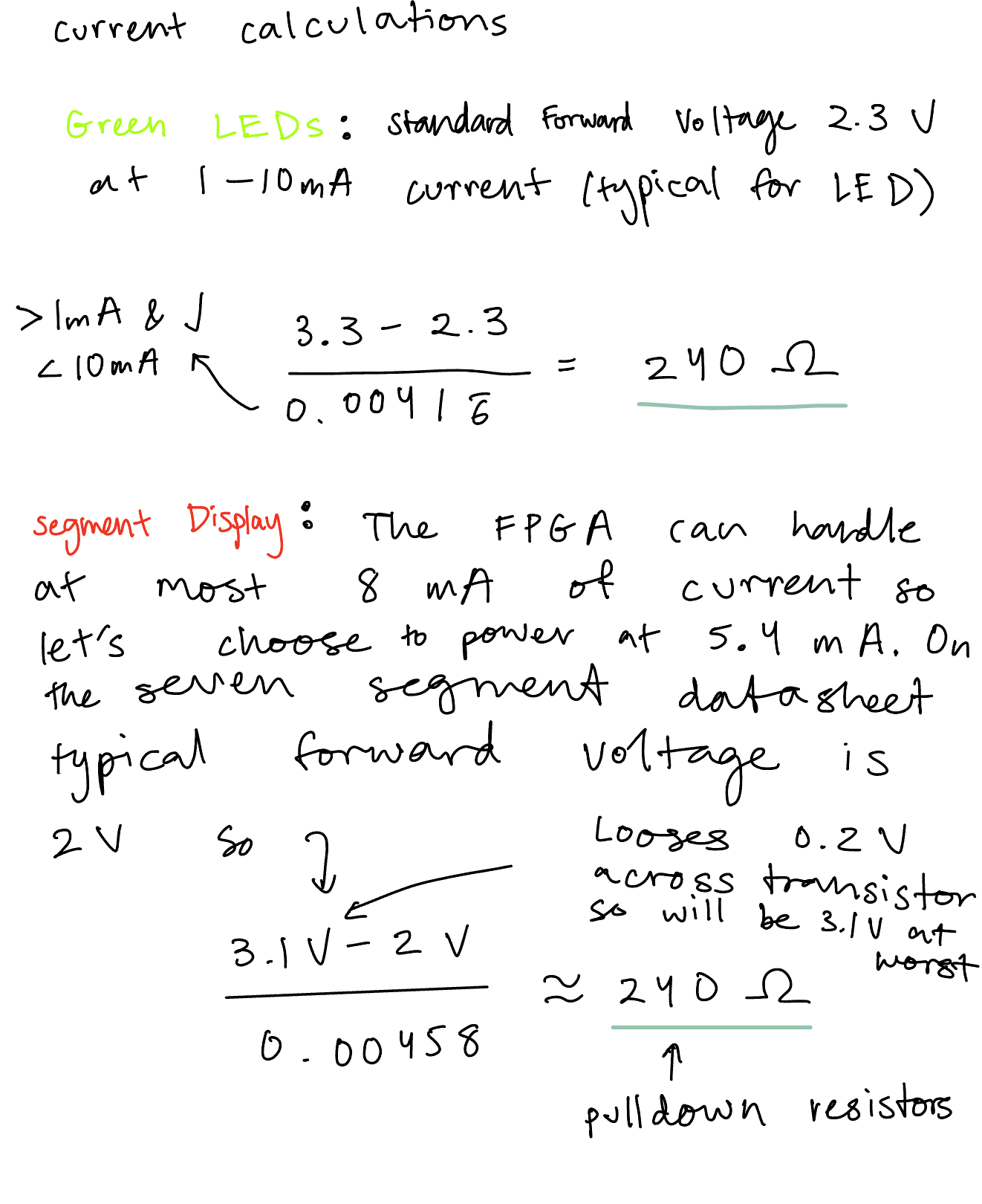
Current Calculations
I also used known values and datasheets to calculate all the resistor values for the LEDs, PNP Transistors, and Dual Seven Segment Display. See the calculations below in Figure 1.

Technical Documentation
All the code for the project can be found in the following Github repository.
Block Diagram
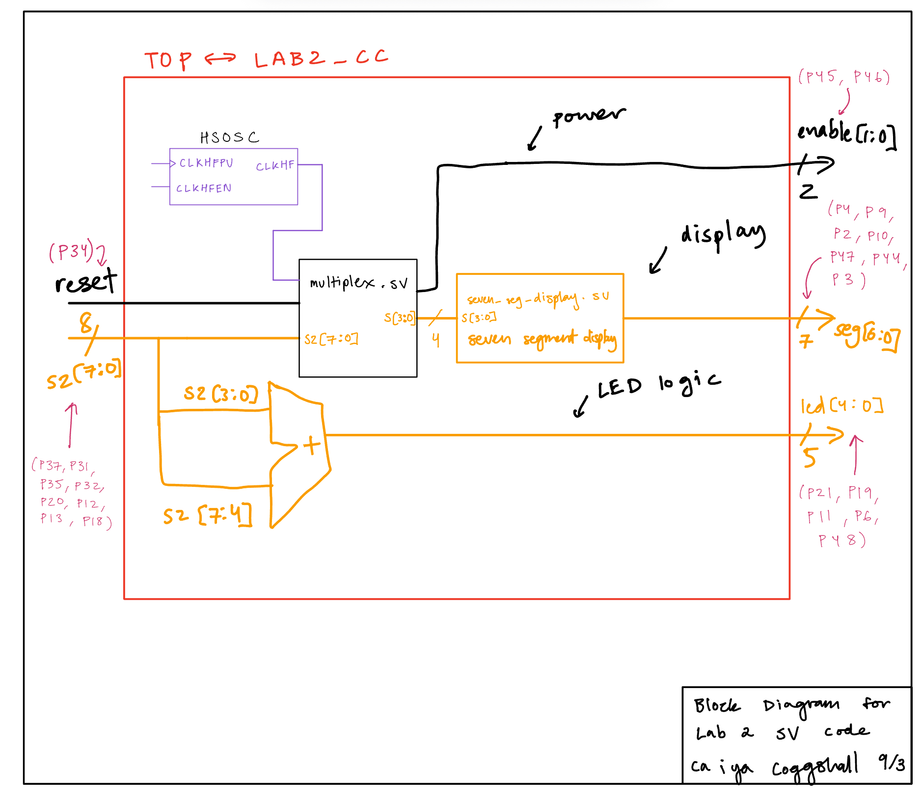
The block diagram in Figure 2 demonstrates the overall architecture of my design. I had three main modules, one for my multiplexer code (i.e choosing which input and power to turn on), one for my seven segment code (i.e telling which segments to light up based on input), and the top module containing everything as well as the high speed oscillator andcombinational LED logic.
Schematic
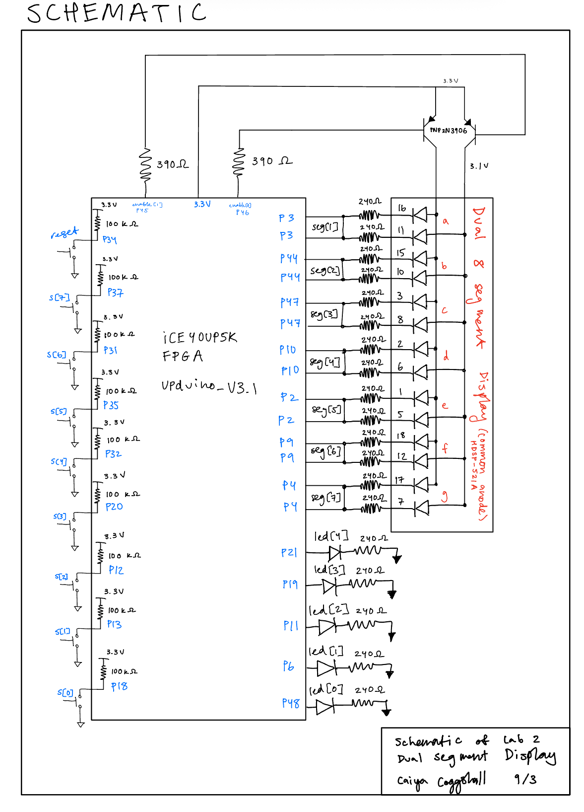
The schematic as seen in Figure 3 shows the layout of the circuit design. It has internal 100 kΩ pullup resistors to make sure the active low reset pin doesn’t float and then the output LED and PNP transistors were connected to a current limiting resistor to make sure the output current didn’t exceed the max output current of the FPGA I/O pins. With the connection from the FPGA to the Dual Seven Segment Display, I could have wired the board with only 7 resistors and it would have worked just as well but this method was slightly more intuitive and so what I choose to go with. Refer to Figure 1 for resistor calculations.
Results and Discussion
After many hours of writing code and debugging I was able to write testbenches using assert statements that produced all correct waveforms. The design met all intended design objectives as seen by the figures below!
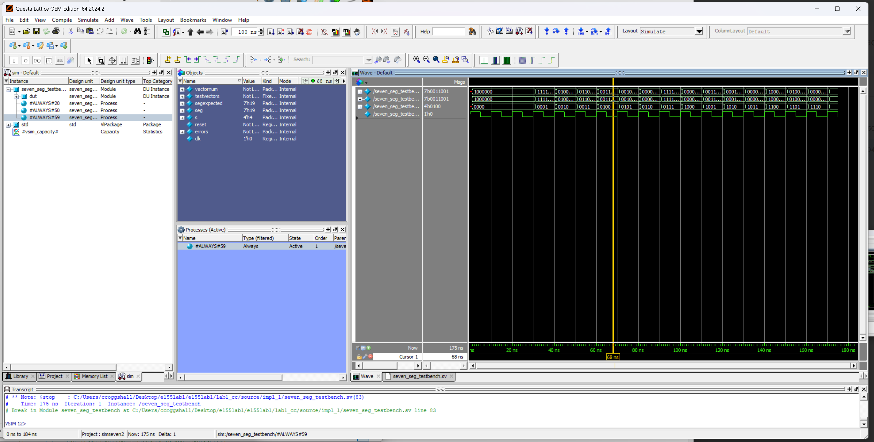
Figure 4 shows the seven_seg_display HDL module works against the test vectors I wrote.

Figure 5 shows that the top down HDL module and confirms the combinational LED logic works because it’s the sum of the two 4 bit DIP switch inputs represented in an 8 bit variable scounttop. This testbench cycles through all possible scounttop numbers.
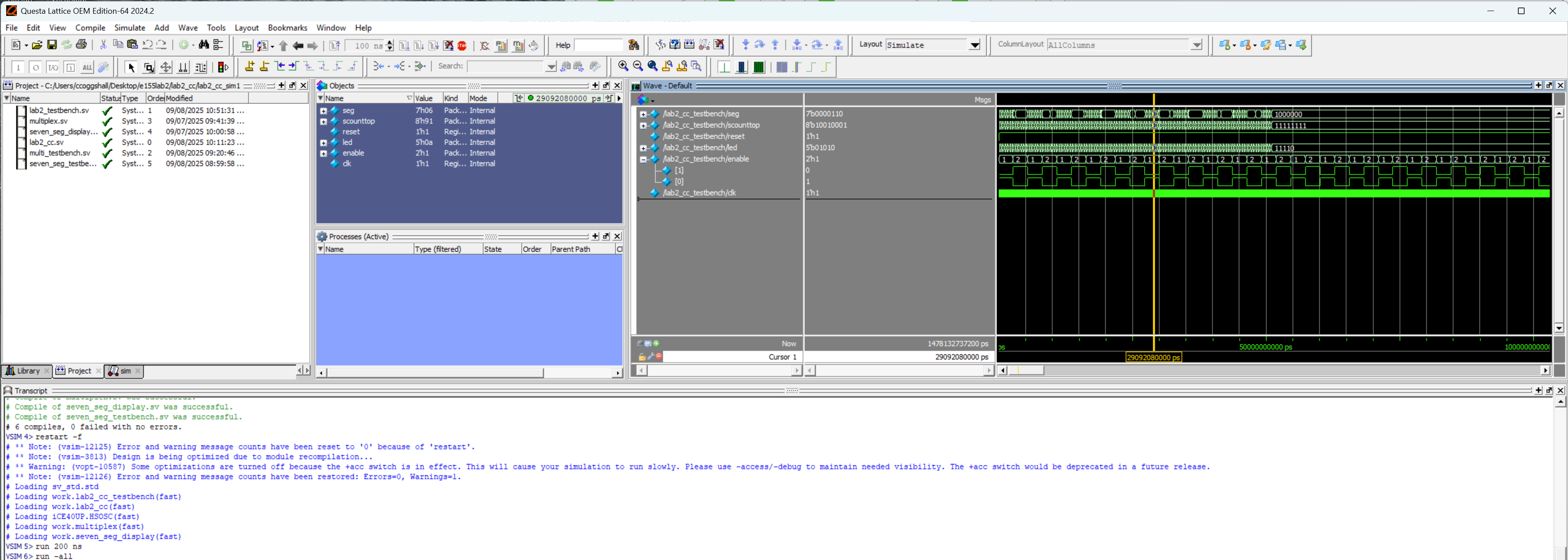
Figure 6 shows the top down HDL module again but this time across a longer time period to show that the enable does toggle between it’s ON states.
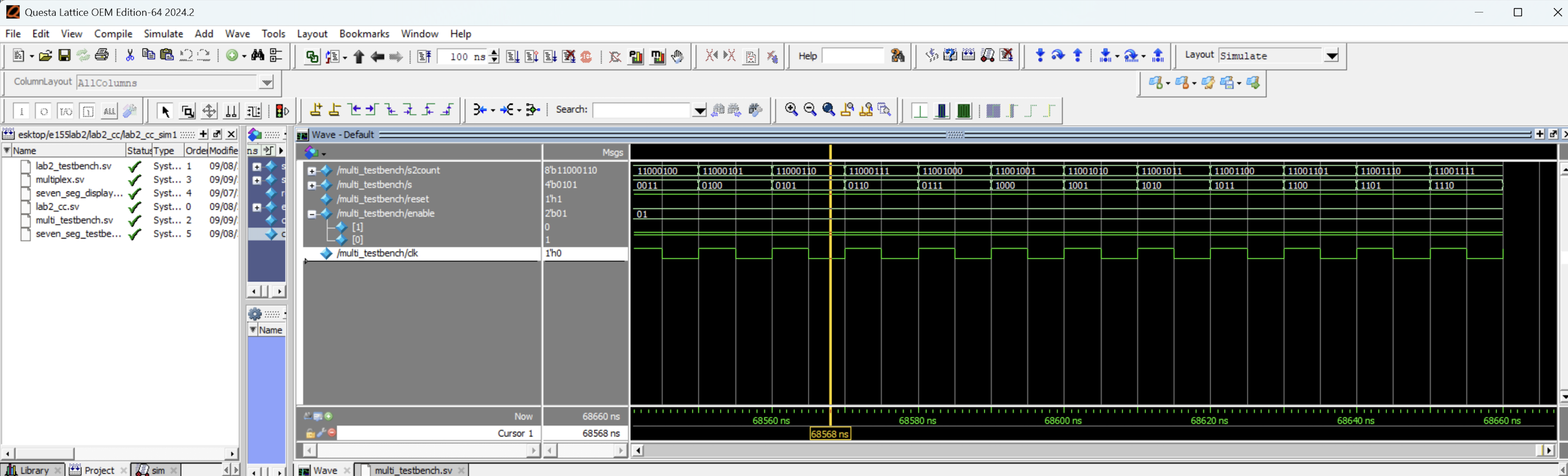
Figure 7 shows the multiplex HDL module working where s receives either the front 4 bits or back 4 bits of s2count on the next clock cycle. This makes sense because in the test bench I’m setting the 8 bit input and instantiating my multiplex HDL module code on that clock cycle. So on the next clock cycle I get an s output from my multiplex code while my s2count increments to a new number. This is explains the 1 cycle mismatch on the waveforms.
Also, this image shows that it get’s the correct 4 bits of s2count because in this image enable[0] is ON and enable[1] is OFF which means that s2count is receiving bit’s [3:0] which is what we see on the waveform.
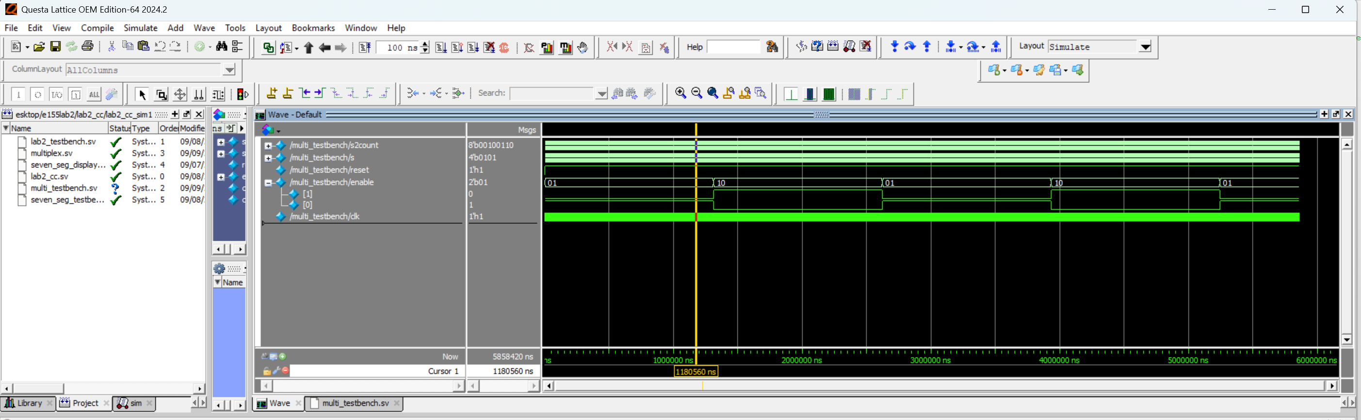
Figure 8 shows Figure 7 again but run for a longer time period to show the enable toggling.
Conclusion
Total Hours Spent on Lab: 27 hours
The lab still took quite a long time to complete but it did reduce significantly when compared to Lab 1. Additionally, all of the hardware and testbenches work so I was very happy about that!
Here’s a video of the working Dual Seven Segment Display!
AI Prototype Summary
I used ChatGPT 5 Auto as my LLM for this assignment. I then entered in the following prompt:
"Write SystemVerilog HDL to time multiplex a single seven segment decoder (that decodes from four bits to a common anode seven segment display) to decode two sets of input bits and drive two sets of seven output bits."This produced the following code blocks that synthesized first try:
// 4-bit hex to 7-seg decoder
// seg[6:0] = {a,b,c,d,e,f,g}, ACTIVE-LOW for common-anode displays.
module sevenseg_decode_hex_ca (
    input  logic [3:0] d,
    output logic [6:0] seg
);
    always_comb begin
        unique case (d)
            4'h0: seg = 7'b0000001; // 0
            4'h1: seg = 7'b1001111; // 1
            4'h2: seg = 7'b0010010; // 2
            4'h3: seg = 7'b0000110; // 3
            4'h4: seg = 7'b1001100; // 4
            4'h5: seg = 7'b0100100; // 5
            4'h6: seg = 7'b0100000; // 6
            4'h7: seg = 7'b0001111; // 7
            4'h8: seg = 7'b0000000; // 8
            4'h9: seg = 7'b0000100; // 9
            4'hA: seg = 7'b0001000; // A
            4'hB: seg = 7'b1100000; // b
            4'hC: seg = 7'b0110001; // C
            4'hD: seg = 7'b1000010; // d
            4'hE: seg = 7'b0110000; // E
            4'hF: seg = 7'b0111000; // F
            default: seg = 7'b1111111; // all off
        endcase
    end
endmodule
and
// Time-multiplex a single decoder across two inputs and drive two outputs.
// Common-anode (active-low) segments on seg0[6:0] and seg1[6:0].
module two_digit_mux_from_one_decoder #(
    parameter int CLK_HZ      = 50_000_000, // input clock frequency
    parameter int REFRESH_HZ  = 1000        // per-digit refresh rate (~flicker-free)
) (
    input  logic        clk,
    input  logic        rst_n,        // active-low reset
    input  logic [3:0]  nibble0,      // left (or digit 0) input
    input  logic [3:0]  nibble1,      // right (or digit 1) input
    output logic [6:0]  seg0,         // segments for digit 0, active-low
    output logic [6:0]  seg1          // segments for digit 1, active-low
);

    // Divide clock so we toggle which digit we service at ~REFRESH_HZ.
    // Because we service one digit per toggle, overall full cycle per digit is REFRESH_HZ.
    localparam int TICKS_PER_TOGGLE = CLK_HZ / (REFRESH_HZ * 2);
    localparam int CNTW             = (TICKS_PER_TOGGLE > 1) ? $clog2(TICKS_PER_TOGGLE) : 1;

    logic [CNTW-1:0] div_cnt;
    logic            sel;       // 0 -> service digit0 this slice, 1 -> digit1

    always_ff @(posedge clk or negedge rst_n) begin
        if (!rst_n) begin
            div_cnt <= '0;
            sel     <= 1'b0;
        end else begin
            if (div_cnt == TICKS_PER_TOGGLE-1) begin
                div_cnt <= '0;
                sel     <= ~sel;
            end else begin
                div_cnt <= div_cnt + 1'b1;
            end
        end
    end

    // Single shared decoder instance
    logic [3:0]  cur_nibble;
    logic [6:0]  seg_decoded;

    always_comb begin
        cur_nibble = (sel == 1'b0) ? nibble0 : nibble1;
    end

    sevenseg_decode_hex_ca u_dec (
        .d  (cur_nibble),
        .seg(seg_decoded)
    );

    // Latch the decoder output into the corresponding digit's segment register
    // on each time slice. Each output holds its last computed value while the
    // other digit is being serviced.
    always_ff @(posedge clk or negedge rst_n) begin
        if (!rst_n) begin
            seg0 <= 7'h7F; // all off (active-low)
            seg1 <= 7'h7F; // all off
        end else begin
            if (sel == 1'b0) begin
                seg0 <= seg_decoded;
            end else begin
                seg1 <= seg_decoded;
            end
        end
    end

endmodule
I started a new conversation and entered the following prompt, now with my own files:
"Write SystemVerilog HDL to time multiplex a single seven segment decoder (that decodes from four bits to a common anode seven segment display) to decode two sets of input bits and drive two sets of seven output bits. Use the seven segment decoder and oscillator provided in the attached files."The code it produced was the following:
// ===============================================================
// Dual 7-seg time-multiplex core (uses a single decoder instance)
// ===============================================================
module dual_sevenseg_mux_core #(
    // Choose which counter bit to use for refresh.
    // With an ~48 MHz HFOSC, REFRESH_BIT=15 gives ~1.46 kHz toggle (~730 Hz per digit).
    // You can tune this as needed; anything ~200 Hz–1 kHz per digit looks steady.
    parameter int REFRESH_BIT = 15
) (
    input  logic        clk,
    input  logic        reset,       // async or sync is fine; used synchronously below
    input  logic [3:0]  a,           // first  digit value (0..F)
    input  logic [3:0]  b,           // second digit value (0..F)
    output logic [6:0]  seg_a,       // 7-seg bus for digit A (common-anode, active-low)
    output logic [6:0]  seg_b        // 7-seg bus for digit B (common-anode, active-low)
);

    // ----------------------------------------------------------------
    // Refresh divider: toggles which digit is active
    // ----------------------------------------------------------------
    logic [REFRESH_BIT:0] div;
    always_ff @(posedge clk) begin
        if (reset) div <= '0;
        else       div <= div + 1'b1;
    end
    logic sel;                // 0 => drive A, 1 => drive B
    assign sel = div[REFRESH_BIT];

    // ----------------------------------------------------------------
    // Single shared decoder
    // ----------------------------------------------------------------
    logic [3:0]  nibble_mux;
    logic [6:0]  seg_decoded;

    always_comb begin
        nibble_mux = (sel == 1'b0) ? a : b;
    end

    // Your provided decoder (common-anode, active-low segment map)
    seven_seg_display ssd_inst (
        .s   (nibble_mux),
        .seg (seg_decoded)
    );

    // ----------------------------------------------------------------
    // Gate the outputs: one bus shows the decoded pattern while the
    // other is driven "all off" (all 1's for common-anode).
    // ----------------------------------------------------------------
    always_comb begin
        // default = OFF
        seg_a = 7'b111_1111;
        seg_b = 7'b111_1111;

        if (sel == 1'b0) begin
            seg_a = seg_decoded;     // show A
        end else begin
            seg_b = seg_decoded;     // show B
        end
    end

endmodule


// ===============================================================
// Example top: instantiate on-chip HFOSC, then the core above
// ===============================================================
// If your flow already provides a clock (or if you have a different
// oscillator wrapper), you can skip this top and hook the core up from
// your own top-level.
//
// Notes for iCE40 UP5K:
// - SB_HFOSC is the built-in high-frequency oscillator primitive.
// - CLKHF_DIV parameter controls the internal divisor (00=48 MHz, 01=24 MHz, 10=12 MHz, 11=6 MHz).
// - Drive CLKHFEN=1 and CLKHFPU=1 to enable and power up the oscillator.
module top_dual_sevenseg (
    input  logic       reset,     // active-high
    input  logic [3:0] a,
    input  logic [3:0] b,
    output logic [6:0] seg_a,     // to 7-seg A (common-anode, active-low)
    output logic [6:0] seg_b      // to 7-seg B (common-anode, active-low)
);
    // -------------------------
    // On-chip HF oscillator
    // -------------------------
    logic clk_hf;

`ifdef ICE40
    // Lattice iCE40 HFOSC primitive
    SB_HFOSC #(
        .CLKHF_DIV("0b00") // 48 MHz
    ) u_hfosc (
        .CLKHF   (clk_hf),
        .CLKHFEN (1'b1),
        .CLKHFPU (1'b1)
    );
`else
    // If you’re simulating or targeting a different device, replace this with your board clock.
    // For sim, you can drive 'clk_hf' from a testbench.
    // synthesis translate_off
    initial clk_hf = 1'b0;
    always #10 clk_hf = ~clk_hf; // 50 MHz sim clock
    // synthesis translate_on
`endif

    // -------------------------
    // Multiplexing core
    // -------------------------
    dual_sevenseg_mux_core #(
        .REFRESH_BIT(15)   // tune as desired
    ) u_mux (
        .clk   (clk_hf),
        .reset (reset),
        .a     (a),
        .b     (b),
        .seg_a (seg_a),
        .seg_b (seg_b)
    );

endmodule
This one got an error on the first synthesis for instantiating an unknown module (seven)_seg), which actually just ened up requiring me to add my Lab 1 seven_seg_display.sv HDL module into the project and then it worked!
This is all to say it’s honestly a little frustrating that AI is able to get the code so fast because it feels like it devalues all the time I spend on the code for the lab. However, I will say (and this may be from my lack of SV knowledge), a lot of the code isn’t the most intuitive to me.
One thing I do take away from the code, is that AI tends to break up the code into more modules than I do which keeps its code organized. Aditionally, I like how it wrote the seven segment always_comb logic with hex numbers. The active-low and active high reset for the digits was very smart and made the logic much more simple too. This is all to say that given the minimal errors and generally looking through the code, AI is able to produce a very good model and there’s a lot to be learned from how it’s code is being structured.